
This dual-layer composite SMT wave soldering fixture uses stacked composite plate construction with side support brackets. Multi-cavity layout accommodates irregular PCB shapes while maintaining high rigidity during wave soldering cycles.
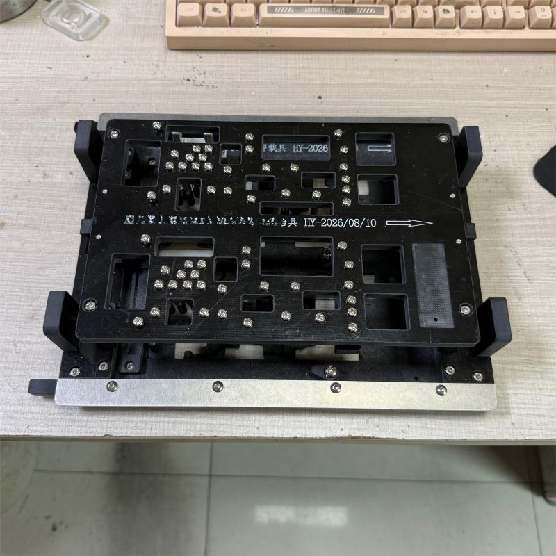
This dual-layer composite SMT wave soldering fixture adopts stacked high-temperature composite board structure. The dual-layer design delivers higher rigidity than single-layer composite plates, effectively reducing board bending when processing complex irregular PCBs. Custom multi-cavity cutouts are precision CNC machined to match unique PCB outlines. Side reinforced support brackets protect the fixture edges from collision on the SMT conveyor. Multiple positioning studs secure the PCB flat and prevent shifting during tin wave contact. The composite material maintains stable dimension under repeated thermal shock. Laser marked part number and production date on fixture surface for easy product identification in the workshop. This design is well suited for irregular outline PCBs with mixed SMD and through-hole components.
Key Features
- Dual stacked composite plate structure, higher rigidity than single layer composite jig
- Side reinforced support brackets, anti-collision during transportation on SMT conveyor
- Custom multi-cavity cutouts for irregular shaped PCB
- Laser engraved part marking for quick workshop identification
Applications
- Complex & irregular outline PCB wave soldering
- SMT assembly with mixed SMD and through-hole components
- Mid volume electronics manufacturing wave soldering lines
FAQ
Q1: What is the advantage of dual-layer composite versus single composite plate?
A1: Dual-layer structure improves overall rigidity, reduces thermal bending for large or irregular PCB carriers.
Q2: Can we modify the cavities if our PCB design is updated later?
A2: The upper composite layer can be reworked or replaced separately when PCB outline changes.